S100 Computers

Home S-100 Boards History New Boards Software Boards For Sale
Forum Other Web Sites Quiz Index    
  
An IDE drive Interface Board

History of the IDE Interface.
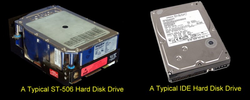
Most later S-100 users have some kind of hard disk system to store and retrieve data.  In the early 1980's the so called "Winchester"  ST-506 drives were by far the most commonly used drives.

The ST-506 was the first 5.25 inch hard disk drive. Introduced in 1980 by Seagate Technology (then Shugart Technology), it stored up to 5 megabytes after formatting. With the ST-506 interface, the drive was connected to a controller card with two cables and power. The drives were "dumb",  because the control card had to translate requests for a particular track and sector from the host system into a sequence of head positioning commands, then read the signal from the drive head and recovered the data from it. 

A number of other companies quickly introduced drives using the same connectors and signals, creating a ST-506-based hard drive standard. IBM chose to use it, acquiring adapter cards for the PC/XT from Xebec and for the PC/AT, from Western Digital. As a consequence of IBM's endorsement, most of the drives in the 1980s were ST-506-based. However the complexity of the controller and cabling soon led to newer solutions like SCSI, and later, IDE.
 
 IDE & ST-%)^ drives

The IDE drive interface itself has a long history of incremental technical drive interface developments over the years. IDE evolved initially from Western Digitals hard drive interface used in the above  IBM-AT.  The central idea of the IDE interface was to place the drive controller, data separator etc. on the drive itself. This was a major improvement over the earlier ST-506 interfaces.  It allowed for more drive construction possibilities, better standardization, better reliability and a more flexible connection to the computer itself.  There were a number of improvements and name changes occurred over the years such as ATA/ATAPI.  After the market introduction of Serial ATA in 2003, IDE/ATA interfaces were retroactively renamed Parallel ATA.  I shall still use the term IDE here.

There are now actually two types of IDE connectors the "standard' 40 pin connector found on all IBM-PC type motherboards  and a newer 44 pin connector used mainly in laptops for small laptop drives. The extra 4 pins are used to bring power (+5V) to the drive.  Here is a picture of a standard IDE connector:-

IDE Connector


Introducing a Prototype S-100 Board to Interface with IDE Drives.
In the early 80's I too, used an ST506 hard disk drive. My initial drive was a Shugart 5Mg drive. Later I moved to a larger drive with both CPM and DOS partitions. The S-100 controller board I use is the Xcomp dual S-100 boards.  I will write-up a description of this board and describe the software at a later stage.

Here I wish to describe a S-100 prototype board I constructed that allows one to interface the S-100 bus with a standard IDE drive interface.  This increases tremendously the range of drives you can use to run CPM, CPM86 and MS-DOS with on the S-100 bus.  Since the typical capacity of a CPM system is up to 8MG capacity, almost any old IDE drive is suitable.

Of particular usefulness is the ability to use IDE to Compact Card Flash memory cards with this board.  This allows you to have a modern solid state drive on your S-100 system booting CPM silently and almost instantly. Here is the actual pinouts of a CF drive.  There are many "IDE adaptors" available for a few $ that allow you to read and write to a CF card over an IDE connection. We will use them here.

The basic concept is to interface to the IDE drive(s) using a simple 8255 parallel IO chip.   This was one of the workhorse parallel port LSI chips of the 70's. It contains 3 parallel ports which can be input, output, or bi-directional. The chip takes up only four I/O ports, one for control, three for the data.   Programming the 3255 is a little tricky because it is an extremely powerful chip.  There are many articles in the literature describing how to do this. The best is a book by Paul F. Goldsbrough "Microcomputing Interfacing with the 8255 PPI Chip", Howard Sams, 1979. 

There was a pivotal article for interfacing an IDE drive written by Peter Fassee in 1998 where he interfaced an IDE drive using a 8255 with a 63B03 CPU. It can be seen here.  This was further elaborated upon by a number of others over the years to work with other CPU's, for example an 8051 CPU, see here, (Both articles can be located on the great web site for such things at www.pjrc.com).  However I have not seen a layout for the S-100 bus with a Z80 CPU.  That is what we have here. 

What is most striking about the IDE interface when we compare it to the ST506 interface is how simple the software and hardware is. With the exception of the actual sector read and write commands of raw data, all commands are 8 bits. You simply setup the drive controller for a particular head, track and sector number. Then pulse a read or write signal and the drive delivers 512 bytes of data.  For the real die hard's, the IDE specs can be seen here.  The only complication is as Peter Fassee pointed out the switching of I/O modes in the 8255. In order to prevent glitching of signals, some lines on port C of the 8255 need to be inverted. See the above articles for more information.

The prototype board layout was fairly straightforward and can be seen b
elow.  Since there is plenty of room on the board I like to use plenty of diagnostic LED's to see what is going on.  A full IEEE-696 addressing scheme of 24 address lines and full 16 bit (or just 8 bit) port addressing will be added to the final board (see below). 

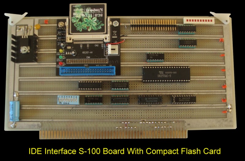
Here is a picture of the prototype board:-

IDE 8255 Prototype Card

This was my test system to debug the software. It used only 8 bit IO address decoding.  The board has a standard IDE 40 pin connector at the top right hand side to hook-up to an IDE hard disk via a standard drive cable. Also on the board is connection to an IDE to CF flash card "adaptor".  Today these "adaptors" are numerous, some costing as little as $8. I soldered the above card directly to the board using the adaptor cards protruding pins at the back of the CF IDE socket.  Other cards have a male IDE pins that can attach to the board IDE pins if they are right angled.  The LED readout in the above diagram is such that when everything is functioning normally they should all be lit (for the master drive).
 

Diagnostic Software
The board can be tested with a short diagnostic program (MYIDE.ASM) I wrote which can be seen  here
The MYIDE.ASM file can be downloaded here:- MYIDE.zip

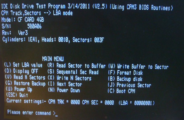
Here is how the program looks when it first comes up. 

MYIDE Signon

First a few comments on the code. 

You must set the equates for the 4 ports of the 8255 LSI I/O chip. They must be contiguous. I use ports 30H-33H.  Next you need to set the MAXSEC equate to the maximum number of sectors/track for your drive. This is typically written on the drive label itself.  Since CPM systems will typically only utilize a fraction of a modern IDE drive if in doubt use a low number of sectors/track. 
 
The next issue is how are you going to communicate with the keyboard/CRT/LCD display.  If the equate for CPM=TRUE, communications will be via standard CPM/BDOS calls.  However in cases where you do not yet have CPM up and running, if the CPM equate is set to FALSE, output will go to directly your consol ports. These need to be set to their correct values. The code is very simple and straightforward. Its menu driven. 

The program on starting reads the disk parameters and displays them. It then presents a short list of menu items.
 
Only the (L)BA menu item perhaps needs explaining.  In the early days of IDE drives, sectors were defined in terms of tracks, sectors and heads. Sectors were a 16 bit number, tracks were a 32 bit number, and heads were a 4 bit number.  This lead to incompatibility amongst drives with different numbers of sectors/track, or heads /drive. Software "drivers" had to be tailored to each drive.   The MYIDE program can easily be modified to talk to the disk in this format. However these drives are really no longer used.  Instead a "Logical Block Addressing" or LBA mode was developed.  Here we address all sectors on the drive as 0 to the maximum number of sectors on the drive as one 24 bit number.  We let the drive electronics figure out the actual track, sector and head.  Unfortunately as we shall see later CPM still thinks in terms of tracks and sectors. So we must convert our CPM type sector/track request to a LBA sector request for the drive. 
 
With the
"L" command you enter a two hex digit sector number, a 2 digit hex high track number and then a 2 digit Hex low track number (tracks are 16 bits).For example 00,02,00 would give the first sector on track 2 (in CPM terminology) of the drive.  The actual LBA number for my drive turns out to be 0000201H. You then hit "R" to read that sector. Then "D" will toggle a detailed display of the sector contents  (@ 3000H in RAM) in hex.  The "S" command will sequentially read one sector after the next continuously over the whole disk. A good way to be sure your hardware is sound. 
 
The
"W" command writes 512 bytes of whatever is in RAM at 3000H to a specified sector. Use with care!  The "N" stops the drive spinning, the
"U" command starts it up again. The "F" command formats each sector with "E5's".  This is necessary to have an empty directory the first time you use the disk with CPM.   MS-DOS/Windows does not do this the same way. Finally while you probably could write a format program to format these drives. I find it easier to pop them into a PC, Format them under windows in FAT32 mode and use them directly in my system.  To avoid CPM's directory getting confused, I have a sector write command that writes 0E5's in sectors  under the (F)format command in MYIDE.COM . You only need the first few tracks of course. To be on the safe side I always erase *.* with a new drive with CP/M anyway.  The above of course is a one time only event. After that the drive can be treated like any other CPM drive.  I have not used this board with MS DOS yet.

The
"V" and "X" command allow you to rapidly read/write a block of sectors. This with care can be used to write/copy CPM system images to/from the system tracks. The "B" and "G" commands allow you to backup/restore the complete CPM disk image (8MG) to another location on the drive/CF card.  Finally the "C" allows you to boot the CPMLDR file on the system tracks of the disk (if it is present).  Some block moves in the code there since the CPMLDR must reside at 100H in RAM!


A Production Board
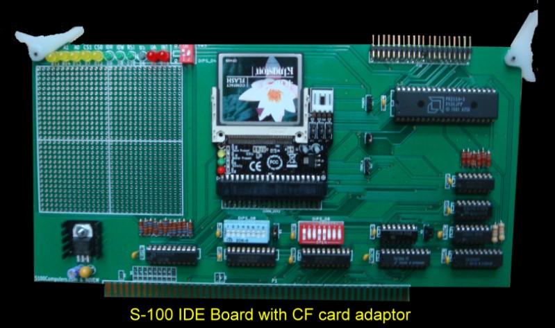
Because this board and software may be of use to others and because I would like to have a "real" board rather than the above prototype in New Boards, together with Andrew Lynch at N8VEM (see here) we made a "proper" commercial type S-100 board.  Through Andrew's magic hands (and hard work) a very nice S-100 board has emerged.  Shown below. The board uses 24 bit address lines and 16 or 8 bit IO ports.
   
IDE Board Final

Here is a detailed schematic of the board.  If you have an interest in such a bare board, let Andrew or I know. We made an initial batch of 20 boards (for $20 each). These are all now gone. If there is enough interest another batch will be made.  This clearly applies only to people who know what they are doing and can splice in a CPM, CPM3 or DOS BIOS  driver to their system.  I have opened up a forum entry for questions and comments about this board here

Help Building The Board
Should you decide to build a board like this yourself, here are some useful tips and step by step instructions in doing so.

First install the voltage regulator and power supply capacitors. Make sure the capacitor on the +8 volts side of the regulator is rated for at least 15 volts. Install all the sockets and filter capacitors, resistors and LED's. For the LED's make sure the +5 connection (the longer LED lead) is orientated correctly before you solder it in. Then place the board in a system with an extender card and check the is 5 volts on each and every 20 pin and 14 pin socket (pins 20 & 14).  Check pin
26 of the 8255 socket also is +5 volts. Carefully inspect each solder joint and make sure it is correct. There is a great ground plain on this board, however this causes the ground pin pods for each socket have heat conducted away well when soldering. I sometimes find it hard to get a good joint. I had one case where the board LED's worked fine only if the board was flexed. It later turned out to be a bad ground pin solder joint I did.

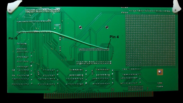
Unfortunately there was a slight error in the board's manufacture that requires a single jumper wire be connected from pin 18 of the 8255 (U8) to pin 4 of the connector P42.  The picture below shows the back of the board with this long wire jumper. Make sure you use the correct P42 pin. It's the second pin in top row of pins.

Back Wire Jumper

Next install the two switches and only U2 and U3.   We now will check port addressing. The board utilizes 74LS682's for port addressing. If your are unfamiliar with this technique click here.

Let’s assume you will be using the 4 port block 30H to 33H. This is what I have the diagnostic software (MYIDE.ASM) port defaults.  We will set the 16 bit I/O address range to 00xxH by jumpering K5 to 1-2 (the top two positions). Set switch SW2 positions 1-8 to closed. Set switch SW1 to 30-34H by having the switches (left to right):-
Open, closed, closed, open, open, closed, closed, closed.
  
Now put the card in your S-100 extender card and start the computer.
With your monitor at 0H in RAM enter:-
DB, 30, C3, 00, 00
Jump to 0H. With a probe you should have pin 19 of U2 pulse continuously.  Do not go further until you see this.
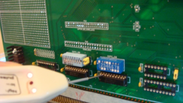
IDI Probe picture

Next add all the other IC’s except the 8255, U7 and U9.  Note, U4 MUST be a 74H04 or 74S04 (see below). The board will not work with IDE/CF cards with a 74LS04. (It seems to be OK for slower Hard Disks with a 74LS04 chip).
 
Repeat the above software test. Check that pin 1 & 19 of empty socket of U9 for a pulse. It should not pulse for any other value except 30H, 31H, 32H, & 33H. This insures we are able to read the data port correctly. Now the write to ports test.

Same software as above except we have:-
D3, 30, C3, 00, 00
Check for a pulse on pins 1 & 19 of empty socket U7.  Again it should not pulse for any other value except 30H, 31H, 32H, & 33H
Only if you get this to work go further.

Insert the two 74LS244’s (U7 & U9) and the 8255.

We will now checkout the 8255. A complex chips with many configuration possibilities/modes.  Fortunately for testing we need only the simplest mode where all 3 ports (A, B & C) are set as simple outputs. To do this from your monitor send to its control port (33H) the byte 80H. With this, port A (30H), port B (31H) and port C (32H) are configured for output ports.

With the LED’s on the board you can easily monitor port A.
Output to port C (32H), 0H.  All the appropriate LED's should come on. Then output 01, 02, 04, 08, 10H, 20H, 40H and 80H. The appropriate LED should go off (see the above schematic).

Next we need to check port A (30H).  Output to port 30H the value 0H.  All the appropriate 8255 pins (4..1, 40..37) should be LOW. Then one at a time output a bit to this port. Starting at bit 0 send 01H to port 30H. See that pin 4 of the 8255 goes high. Continue all the way up to bit 7, pin 37 of the 8255.

Now do the same for the 8255 Port B (31H). First check the pins (18-25).  You will need a copy of the boards schematic. See here.
Output to port 31H the value 0H.  Pins 18-25 of the 8255 should be low.  Output the single bits pattern above and check each appropriate 8255 pin goes high. Only if all of the above checks out should you go further.
 
Next we will check the actual IDE socket pins. Setup the 8255 to all ports output as we did before (Output 80H to port 33H) then output to port 31H the value 0H. ALL appropriate pins, 4,6…18 on any IDE socket should be 0. Then output a 1 to port 31H. ONLY pin 4 on each IDE socket should be high. Same for all the other bits.  Only when you are sure that you can reliably output the correct bit pattern from port 31H of the 8255 to any of the IDE sockets should you go further.

The boards are extremely well made so there is little chance of partial etching. Any stuck bits are probably an error on your part.
 
With the above completed, you are ready to fire things up with an IDE drive. I have used the board with a number of drives and CF cards. I find it is easiest to get things going with an old IDE hard drive.  Be sure you plug you plug the IDE cable in correctly. From the front of the board (V regulators on left) the top IDE socket has pin 1 on the top row at the very right back row of pins.

Download my “MYIDE.ASM” program to check things out.  Run the program under CPM. The drive should come on and display the drive configuration parameters.  See the picture above. The drive I used had 2082 cylinders, 16 heads and 63 sectors/track. You then need to read the sectors/track info you got and if required reassemble the program for your drive with the appropriate equates set in the software. 

As I said, I have two of these new boards running here (on two systems).  They appear very reliable. I have extensively slopped large files to/from memory disks and down to slow floppies. Never a problem. It’s so nice to instantly have CPM3 boot up!
 
The only unusual thing I have found is the requirement of U4 being a fast 74H04 or 74S04 when using CF disks.  It’s an absolute requirement for the cards I have. Not so for regular hard disks.  I have not really determined why this is the case.

You can "Hot Swap" the CF cards in a running CPM system if you first turn off power to the IDE adaptor/CF  board (SW3), remove the CF card. Insert the new card and THEN turn the power  back on with switch SW3.  With CPM you need to warm boot with a ^C.  Clearly there must be a system on the new CF card or you must do the swap where another drive is the current system drive.


Software
Installing CPM3 On The IDE Disk/Card
In order for this IDE card to be of any practical use we need to install CPM (and later, other disk operating systems) on drives interfacing to it.  We could start with CPM version 2.2, but it is actually easier to write a BIOS for CPM3 because CPM3 takes care of buffer sizes greater than 128 bytes internally (all IDE drive sectors are 512 byte sectors) and is in general is a more practical and expandable system. 

Before writing a CPM3 BIOS for this board please read the write-up I have in the software section of this site about setting up a CPM3 system on a floppy disk system. Please read here first.  Then read here for details as to how to install CPM3 on a drive/CF card using this board.


Update on Version 2 of the S-100 IDE Board.
There was a surprising demand for this S-100 IDE board.  We have now completed a second batch of boards.  These boards are identical to the first batch except the pin 18 to pin 4 dropped trace (described above) has been corrected.   Also on the second batch of boards the "Int" LED does not come on unless the IDE drive request it on its IDE INT line.  Here is a picture of the batch 2 board.

IDE Board V2
  
The schematic for the board can be obtained here, and the board layout here.
 
Two things I forgot to mention earlier when assembling these boards.

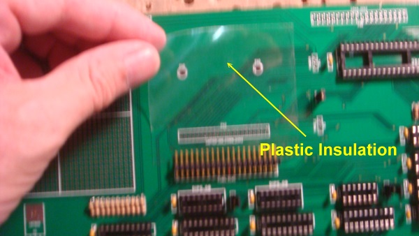
First it is important that the back pins/solder connections of the IDE-Flash Card adaptor do not come in contact with any of the traces on the actual S-100 board.  To be on the safe side I add a layer of adhesive transparent plastic. See this picture:-
 
Plastic Insulation
 
This insures that there will be no connection between the two.

Second, these S-100 boards are of excellent quality and perfectly cut. However the bottom edge where the S-100 connections are is quite square sometimes making it difficult to fit the card into the bus edge connector.   I find it is best to lightly run a file along the bottom front and back of the board to take off the edge  as shown here:-

File At An Angle
 
Please take extreme care not to damage the gold plated connections. The file should be at a 45 degree angle. Two or three sweeps on both sides is all that is needed.

 
A Third Production S-100 Board.
Realizing that a number of people might want to utilize a board like this together with Andrew Lynch at N8VEM (see here) we have now completed a prototype of a THIRD (V2) IDE board. The previous two runs have be used up.

V3 prototype

This board is very similar to the previous boards except that now it has two IDE slots for CF cards instead of one. This allows you to use two separate CF cards in your system. This is very useful for "disk/card" copying and backing up your software.  The board also has an LED HEX display that shows the current sector being read or written to. From a software prospective it is identical to the previous boards.  After a hardware reset the board comes up with the first drive/CF card active with the same software drivers as the V1 board.  The second drive/CF card is set as the current active drive by outputting a bit 0 to the board address port +1.   This way it is very easy to modify your CPM BIOS to address two drives instead of one.

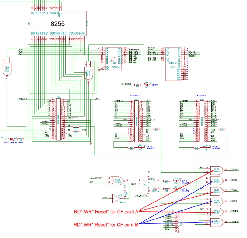
It turned out to be more difficult than I expected to have two CF cards sharing the same IDE "bus".  Normally this bus has a master and a slave drive.  However I could not get both drives to initialize properly. This probably has to do with the fact that the master drive first initializes and only then can one initialize the slave drive. On the web there are references to "interference" in getting two CF drive systems working on the same IDE bus.  In the end I took the simplest approach and setup the system where each drive (thinks) it is a master. This involves sending separate RD*, WR* and Reset* signals to each drive.   A simple 7474 flip flop determines the "active" drive.  Upon reset the first drive/CF card is always the current drive.
Here is the core part of the schematic.

Dual Card Schematic Summary
  
You will also notice I did away with the 74H04 IC. I now understand why that IC was required in the V1 boards.  It turns out the specs for certain signals on an IDE interface require a high signal of 4 volts (CMOS levels).  74LS04 signals could not get to these levels. Presumably the 74H04 signals did.  The spec. requirements are easily met using open collector outputs.  That is why I use 74F03's (actually even 74LS03's are fine) with pull-up resistors in the V2 board.  In a 10Mhz Z80/CPM+ system the board works rock solid with many CF cards (Kingston, Maxell, Patriot etc.). However for some strange reason I could not get it to work with a "Ultra SanDisk 2GB card".  I have not had time to check into this.

Finally, I cannot stress enough the importance of having a clean reset signal to these CF cards. I have not figured out the minimum length of a reset pulse, but here is the code I use for a Z80 running at 10MHz with 2 two I/O wait states. This gives a 60 uS pulse on pin one of the IDE connector and seem to work fine with 5 different CF cards I have.

INITILIZE_IDE_BOARD:              ;Drive Select in [A]. Note leaves selected drive as [A]
        LD       A,RDcfg8255      ;Config 8255 chip (10010010B), read mode on return
        OUT     (IDECtrl),A       ;Config 8255 chip, READ mode
        LD       A,IDEreset       ;IDEreset EQU 80H
        OUT     (IDECport),A
        LD       C,IDE_Reset_Delay ;20 for 10MHz Z80

ResetDelay:
        DEC C
        JP       NZ,ResetDelay    ;Delay (reset pulse width)
        XOR      A
        OUT      (IDECport),A     ;No IDE control lines asserted (just bit 7 of port C)

  
        CALL     DELAY_15         ;Need to wait about 15ms before status is valid
 
              .........

DELAY_15:                         ;DELAY ~15 MS
        LD       A,40
DELAY1: LD       B,0
M0:     DJNZ     M0
        DEC      A
        JR       NZ,DELAY1
        RET


Here is a picture of the signal:-
 
Reset Pulse2


Source Of IDE Adaptors.
Fortunately these single card IDE to CF cards are quite common.  They typically cost ~$10.  
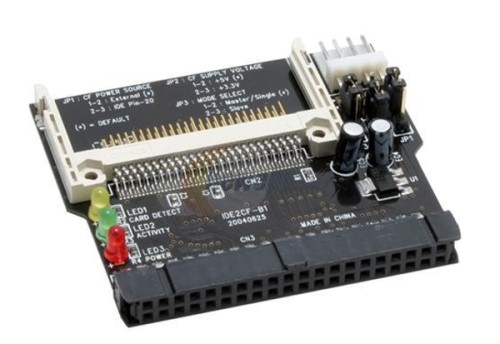
I have been using the SyBA "SD-CF-IDE-DI IDE" adaptor (NewEgg Item# N82E16822998003), shown here:-
 
CF Card Adaptor
  

But there are a number of other types.  For those that may be interested I have tried some dual CF card adaptors (to allow two drives on one adaptor). So far I have not had success with these "dual" CF card adaptors. 


Notes on CHS and LBA Addressing
.
On a PC (at least the early ones),  sectors are defined is terms of Cylinders, Heads & Sectors (CHS format). Parameters in early MS-DOS versions were passed via software interrupt INT 13H for sector reads and writes. INT 13H  designates sectors in a somewhat convoluted way (for historical reasons), parameters passed are always as follows:-
AH = 02h
AL = number of sectors to read/written (must be nonzero)
CH = low eight bits of cylinder number
CL = sector number 1-63 (bits 0-5)
high two bits of cylinder (bits 6-7, hard disk only)
DH = head number
DL = drive number (bit 7 set for hard disk)
ES:BX -> data buffer
Because only 16 heads are allowed with this format, a hard disk can only get to 512MG in size.   This is not a problem for 8 bit CPM systems since disk capacity was always less than 10 MG. To go to higher disk capacities with later version of MSDOS, the PC BIOS's utilized the so called "LBA" sector addressing mode.   In this case sectors are numbered on the disk as just one long number. Starting at 0 and working upwards. There are no tracks or heads. Both formats can be  implemented on our IDE board.

Programming the LED
HEX displays is a little different however for each case.  First the drive must be told what format sectors will be addressed in.  This is done by sending a key bit to the IDE Drive "Head Register".   If bit 6 of this register is set to 0 then the  drive expects all information to arrive in LBA mode.  If bit 6 is a 1, then the drive expects all sector information to arrive in CHS format.
Bit 7 Bit 6 Bit 5 Bit 4 Bit 3 Bit2 Bit 1 Bit 0
Always 1 LBA/CHS mode Always 1 M/Slave Heads 0-15

In the case of LBA addressing, the right most pair of HEX displays are addressed as "Sectors" (0-FFH). The middle pair of displays are addressed as "Low Cylinders" (0-FFH) and the left pair of HEX displays are addressed as "High Cylinders" (0-FFH).  This allows up to FFFFFFH (~16.7 Million) sectors to be identified. BTW, for CPM you need only be concerned with the lower 4 HEX displays, outputting to the IDE drive "Sector" & "Low Cylinder" values.   In any event, either 2 or 3 bytes are sent to the appropriate IDE "registers" via the 8255 port A.

CHS Picture

For CHS addressing we do things the same way, however in this case we need display distinguish the Head register on the  "High Cylinder" HEX display.  The board has a separate access for this display via U12 (74LS244).   We trick the display by first sending head information to the IDE drive via the 8255 port A in the normal way.  We then get the head information to the upper two HEX displays by sending the data to port B of the 8255 and pulsing the IDE High Cylinder line again.  The IDE drive ignores this data on its upper 8 bits data line but the HEX LED displays latch the data. (To illustrate the selected head better I actually put the 4 head bits in the displays high nibble). This may sound more complicate than it is. Please review the 8086 Monitor code (DOS_WR_LBA:) for an example.

If you are sending LBA or true CHS information to a drive for single sector read/writes (e.g. for CPM) it actually does not matter which format the drive uses/expects. In the CHS format there would just be "holes" in the LBA format array.  Where all this becomes critical is when we go to MSDOS where as sector read/write command may require a block of up to 80H contiguous sectors to be processed.  In this case the disk cannot have sector "holes".  When one track of sectors is read the next sector comes from the next head up. When all heads are used only then do we go to the next track.  In any BIOS its critical that this process is toughly tested out.  The software must religiously either follow this process or via a formula translate a LBA address number into a CHS number.  Again please see my 8086 Monitor code  (DOS_WR_LBA:) for an illustration of how this can be done.


A Final Dual IDE Prototype Board
Utilizing all the observations above Andrew and I constructed one more prototype board to make sure everything is correct for what we expect will be a popular S-100 board.  Here is a picture of that board:-
 

IDE Dual Board (Final prototype)

Added where more LED's to let you know which CF card/drive is selected and when a drive is active (RD/WR). The board works fine with 7403's rather than the less common 74F03's. It also works fine with the low power CMOS 82C55's  or the older plain NMOS 8255's. 

It is interesting to go back and see how this board has evolved.   It now has become a fairly sophisticated board and very useful.   These days I store everything on CF cards!
 
If you have an interest in such a bare board, let Andrew  know via e-mail at:-  lynchaj@yahoo.com .
Please note all the above clearly applies only to people who know what they are doing and can  do a little soldering and board assembly.  There will be little hand holding at this stage.

A Production Version of the DUAL IDE Board
Because this board and software may be of use to others, together with Andrew Lynch at N8VEM (see here) we made a "proper" commercial type S-100 V2 board.   Shown below. The board uses 24 bit address lines and 16 or 8 bit IO ports.  The construction process is more or less the same as that described for the V1 board above, however do consult the schematic as the IC numbers etc. have changed.  You can see we added a second Voltage regulator. The single regulator was running a little hot on the final prototype. Now the LED HEX display has its own 5V regulator.


IDE Dual Commercial

Source of chips
Most of the IC's use on this board are common 74LSxx chips available from numerous sources such a Jameco, Mouser & DigiKey. 

The TIL 311A's are expensive (~$20 each from places like Jameco).  However overseas outfits like Utsource sell them in small quantities for ~$5 each. Utsource have about a 1 week delivery time to the US since they use DHL.  It is indeed frustrating these LED HEX displays are so expensive. With the exception of the even rarer HP-5082's other such displays display only the digits 0-9.  An alternative approach would be to use a 7 segment LED decoder such as a DM9368 and a simple 7 segment LED display. However these too are no longer normally stocked.  Normal single line flat panel LCD displays just do not show up well when the card is in the S-100 bus card cage.

The links below will contain the most recent schematic of this board.
Note, it may change over time and some IC part or pin numbers may not correlate exactly with the text in the article above.

MOST CURRENT IDE BOARD SCHEMATIC (V2-C2, FINAL,  6/12/2011)
MOST CURRENT IDE BOARD LAYOUT  (V2-C2, FINAL, 6/12/2011)

MOST CURRENT PARTS LIST  (V2-C2, FINAL, 6/12/2011)

An updated version of the diagnostic program can be seen here and downloaded here. (7/10/2011)
A 4K ROM based version of MYIDE.ASM can be see here and downloaded here. (3/15/2011)
A CPM3 BIOS using this card is described in detail here. (3/15/2011)

Other pages describing my S-100 hardware and software.
Please click here  to continue...


This page was last modified on 09/18/2011